- 您现在的位置:买卖IC网 > Sheet目录3761 > ATMEGA324A-MCHR (Atmel)IC MCU AVR 32K 20MHZ 44QFN
131
8272E–AVR–04/2013
ATmega164A/PA/324A/PA/644A/PA/1284/P
Using the ICRn Register for defining TOP works well when using fixed TOP values. By using
ICRn, the OCRnA Register is free to be used for generating a PWM output on OCnA. However,
if the base PWM frequency is actively changed by changing the TOP value, using the OCRnA as
TOP is clearly a better choice due to its double buffer feature.
In phase and frequency correct PWM mode, the compare units allow generation of PWM wave-
forms on the OCnx pins. Setting the COMnx1:0 bits to two will produce a non-inverted PWM and
an inverted PWM output can be generated by setting the COMnx1:0 to three (See Table 16-4 on
page 134). The actual OCnx value will only be visible on the port pin if the data direction for the
port pin is set as output (DDR_OCnx). The PWM waveform is generated by setting (or clearing)
the OCnx Register at the compare match between OCRnx and TCNTn when the counter incre-
ments, and clearing (or setting) the OCnx Register at compare match between OCRnx and
TCNTn when the counter decrements. The PWM frequency for the output when using phase
and frequency correct PWM can be calculated by the following equation:
The N variable represents the prescaler divider (1, 8, 64, 256, or 1024).
The extreme values for the OCRnx Register represents special cases when generating a PWM
waveform output in the phase correct PWM mode. If the OCRnx is set equal to BOTTOM the
output will be continuously low and if set equal to TOP the output will be set to high for non-
inverted PWM mode. For inverted PWM the output will have the opposite logic values. If OCR1A
is used to define the TOP value (WGM13:0 = 9) and COM1A1:0 = 1, the OC1A output will toggle
with a 50% duty cycle.
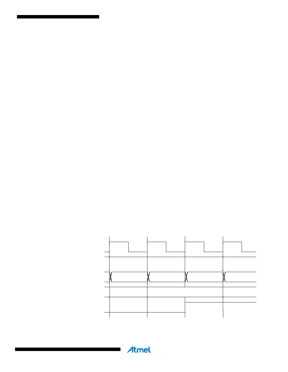
16.11 Timer/Counter Timing diagrams
The Timer/Counter is a synchronous design and the timer clock (clk
Tn) is therefore shown as a
clock enable signal in the following figures. The figures include information on when Interrupt
Flags are set, and when the OCRnx Register is updated with the OCRnx buffer value (only for
modes utilizing double buffering). Figure 16-10 shows a timing diagram for the setting of OCFnx.
Figure 16-10. Timer/Counter Timing diagram, setting of OCFnx, no prescaling.
Figure 16-11 shows the same timing data, but with the prescaler enabled.
f
OCnxPFCPWM
fclk_I/O
2 NTOP
----------------------------
=
clk
Tn
(clk
I/O/1)
OCFnx
clk
I/O
OCRnx
TCNTn
OCRnx Value
OCRnx - 1
OCRnx
OCRnx + 1
OCRnx + 2
发布紧急采购,3分钟左右您将得到回复。
相关PDF资料
XR16L2752CJTR-F
IC UART FIFO 64B DUAL 44PLCC
ST16C650AIQ48TR-F
IC UART FIFO 32B 48TQFP
ST16C552ACJ68TR-F
IC UART FIFO 16B DUAL 68PLCC
ST16C650ACJ44TR-F
IC UART FIFO 32B 44PLCC
XR16V2552IL-F
IC UART FIFO 16B DUAL 32QFN
XR16L2552IM-F
IC UART FIFO 16B DUAL 48TQFP
XR16L2550IL-F
IC UART FIFO 16B DUAL 32QFN
ST16C2552CJ44TR-F
IC UART FIFO 16B DUAL 44PLCC
相关代理商/技术参数
ATMEGA324A-MU
功能描述:8位微控制器 -MCU AVR 32KB FLSH 1KB EE 2KB SRAM-20MHz, IND RoHS:否 制造商:Silicon Labs 核心:8051 处理器系列:C8051F39x 数据总线宽度:8 bit 最大时钟频率:50 MHz 程序存储器大小:16 KB 数据 RAM 大小:1 KB 片上 ADC:Yes 工作电源电压:1.8 V to 3.6 V 工作温度范围:- 40 C to + 105 C 封装 / 箱体:QFN-20 安装风格:SMD/SMT
ATMEGA324A-MUR
功能描述:8位微控制器 -MCU AVR 32KB FLSH 1KB EE 2KB SRAM-20MHz, IND RoHS:否 制造商:Silicon Labs 核心:8051 处理器系列:C8051F39x 数据总线宽度:8 bit 最大时钟频率:50 MHz 程序存储器大小:16 KB 数据 RAM 大小:1 KB 片上 ADC:Yes 工作电源电压:1.8 V to 3.6 V 工作温度范围:- 40 C to + 105 C 封装 / 箱体:QFN-20 安装风格:SMD/SMT
ATMEGA324A-PU
功能描述:8位微控制器 -MCU AVR 32KB FLSH 1KB EE 2KB SRAM-20MHz, IND RoHS:否 制造商:Silicon Labs 核心:8051 处理器系列:C8051F39x 数据总线宽度:8 bit 最大时钟频率:50 MHz 程序存储器大小:16 KB 数据 RAM 大小:1 KB 片上 ADC:Yes 工作电源电压:1.8 V to 3.6 V 工作温度范围:- 40 C to + 105 C 封装 / 箱体:QFN-20 安装风格:SMD/SMT
ATMEGA324P
制造商:ATMEL 制造商全称:ATMEL Corporation 功能描述:8-bit Microcontroller with 16/32/64K Bytes In-System Programmable Flash
ATMEGA324P-15AT
功能描述:8位微控制器 -MCU AVR 32KB 1KB EE 20MHz 2KB SRAM 5V RoHS:否 制造商:Silicon Labs 核心:8051 处理器系列:C8051F39x 数据总线宽度:8 bit 最大时钟频率:50 MHz 程序存储器大小:16 KB 数据 RAM 大小:1 KB 片上 ADC:Yes 工作电源电压:1.8 V to 3.6 V 工作温度范围:- 40 C to + 105 C 封装 / 箱体:QFN-20 安装风格:SMD/SMT
ATMEGA324P-15AT1
功能描述:8位微控制器 -MCU AVR 32KB 1KB EE 20MHz 2KB SRAM 5V RoHS:否 制造商:Silicon Labs 核心:8051 处理器系列:C8051F39x 数据总线宽度:8 bit 最大时钟频率:50 MHz 程序存储器大小:16 KB 数据 RAM 大小:1 KB 片上 ADC:Yes 工作电源电压:1.8 V to 3.6 V 工作温度范围:- 40 C to + 105 C 封装 / 箱体:QFN-20 安装风格:SMD/SMT
ATMEGA324P-15AZ
功能描述:8位微控制器 -MCU AVR 32KB 1KB EE 20MHz 2KB SRAM 5V RoHS:否 制造商:Silicon Labs 核心:8051 处理器系列:C8051F39x 数据总线宽度:8 bit 最大时钟频率:50 MHz 程序存储器大小:16 KB 数据 RAM 大小:1 KB 片上 ADC:Yes 工作电源电压:1.8 V to 3.6 V 工作温度范围:- 40 C to + 105 C 封装 / 箱体:QFN-20 安装风格:SMD/SMT
ATMEGA324P-15MT
功能描述:8位微控制器 -MCU AVR 32KB 1KB EE 20MHz 2KB SRAM 5V RoHS:否 制造商:Silicon Labs 核心:8051 处理器系列:C8051F39x 数据总线宽度:8 bit 最大时钟频率:50 MHz 程序存储器大小:16 KB 数据 RAM 大小:1 KB 片上 ADC:Yes 工作电源电压:1.8 V to 3.6 V 工作温度范围:- 40 C to + 105 C 封装 / 箱体:QFN-20 安装风格:SMD/SMT